
Privacy statement: Your privacy is very important to Us. Our company promises not to disclose your personal information to any external company with out your explicit permission.

Currently widely used DC light-emitting diodes (DC LEDs), if they are to be powered by commercial power, they must be supplied with AC-DC rectifiers, which are likely to cause additional material costs and energy conversion losses. Therefore, the industry has developed direct currents with AC power. Driven high voltage LEDs (HV LEDs) can significantly increase the energy efficiency and luminous efficiency of LED lighting systems.
Among the conventional illumination sources, the luminous efficiency is the best, and the luminous efficiency of the light source itself is about 65 lm/W. The additional circuit for the ballast will cause 13-20% energy loss, and the light source will illuminate through the reflector of the lamp, and the light source efficiency loss is about 30-40%, so in the actual lighting application environment, the lamp illumination of the fluorescent lamp The efficiency is about 35 lm/W. Although the light source itself has high luminous efficiency, the light loss caused by the additional circuit and the lamp structure will greatly reduce the luminous efficiency of the light source.
At present, high-power white light-emitting diodes (DC LEDs) (Table 1) have been widely applied to illumination sources, and their light sources have luminous efficiencies of up to 150 lm/W. However, the DC LED is driven by a DC power supply. If it is to be used in commercial power, it is necessary to add an AC-DC rectifier. The power conversion will cause 20-30% energy loss, and the size of the drive circuit is also Larger, the flexibility of the design of the luminaire will be relatively limited.
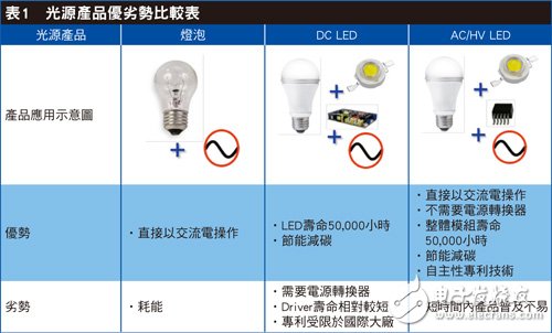
Taiwan's self-developed high-voltage (HV) LED technology products can be directly operated at 110 volts (V)/220V with a simple external drive circuit, and have a 90% high power factor (PF), 95%. High energy efficiency, high luminous efficiency and so on. At present, it has achieved international development opportunities. Domestic manufacturer Jingyuan Optoelectronics has successively shipped HV LED die products to foreign LED packaging and application manufacturers. There are also many related manufacturers in China to invest in HV LED lighting source products. Development is the mainstream trend for future lighting sources.
Different DC LED drive mode HV LED features and design are quite different
The high-voltage LED is a semiconductor manufacturing method in which a plurality of micro-grains are placed on the same substrate and then connected in series, and the required process technology is very similar to that of the conventional LED. However, due to the different driving methods, especially under AC driving conditions, the characteristics and design direction of high-voltage LEDs are significantly different from those of conventional LEDs.
FIG. 1 is a schematic structural view of a high voltage LED chip. A plurality of micro-grains fabricated on the same substrate are connected in series by metal wires, and a high-voltage driving current enters the micro-die strings through the two wire-bonding pads at the ends. From the side view of the micro-grain structure of Fig. 2, the main difference between the structure of the single micro-grain and the conventional LED can be found only in the difference in size, and the other includes the transparent conductive layer, the surface roughening, and the patterned sapphire substrate. Technologies that improve the efficiency of traditional LEDs are equally applicable to high voltage LEDs.
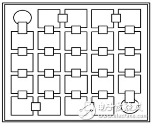
Figure 1 High-voltage LED structure top view
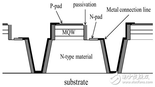
Figure 2 Side view of GaN microcrystals grown on a sapphire substrate
The main differences between the high-voltage LED and the conventional LED chip in the manufacturing process are the use of the insulating substrate, the etching of the insulating trench, and the fabrication of the metal wire. The core concept of high-voltage LEDs is to connect a plurality of micro-grains fabricated on the same substrate in series. Therefore, the use of an insulating substrate to ensure electrical insulation between micro-grains is a basic condition for normal operation of high-voltage LEDs. For LEDs grown with gallium nitride (GaN) materials, since the sapphire substrate used has excellent insulating properties, good electrical properties can be achieved by etching the trenches between the microcrystal grains until the substrate is exposed. insulation.
In addition, it can be seen from FIG. 3 that although the insulating trench between the micro-grains is a necessary structure for the high-voltage LED to operate correctly, the illuminable area of the high-voltage LED chip as a whole is also reduced. Although conceptually, the narrower the insulating trenches can increase the illuminable area of the high voltage LED chip, it also increases the difficulty of the process.
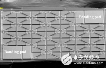
Figure 3 SEM photo of high voltage LED chip
The sidewalls of the insulating trenches shall be covered with a dielectric material to prevent short-circuiting between the PN materials when the metal wires pass through the surface. However, when the insulating trench is too narrow, the film may be incompletely formed by chemical vapor deposition or vapor deposition, and the short-circuit failure of the micro-grain PN material may occur. Similarly, too narrow an insulating trench will make the metal vapor difficult to enter, causing the thickness of the metal wire film to be too thin or even discontinuous, resulting in an increase in the series resistance of the high voltage LED chip, or even an open circuit failure.
In order to improve the process yield of the dielectric material and the wire metal film, it is a feasible way to make the insulating trench into an inverted trapezoidal structure with an opening upward. In addition to the improved sidewall yield of the micro-grain and high-voltage LED, the non-rectangular geometry of the slanted sidewall structure shown in Figure 4 also contributes to the improved light extraction efficiency of the micro-grain. In addition, in order to avoid the metal shielding to reduce the luminous efficiency of the high-voltage LED, the metal wires laid between the micro-grains must have the characteristics of low impedance and low light shielding. Making thin and thick metal wires is one of the methods to achieve the above objectives, and the use of transparent metal oxides such as indium tin oxide (ITO) or zinc oxide (ZnO) as a conductive material is also a feasible means, both of which are feasible. Helps improve the luminous efficiency of high voltage LEDs.
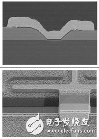
Figure 4 Micro-grain structure with inclined sidewalls and inverted trapezoidal openings
The following is a summary of the HV LED technology research and development at home and abroad.
November 04, 2024
November 12, 2024
البريد الإلكتروني لهذا المورد
November 04, 2024
November 12, 2024

Privacy statement: Your privacy is very important to Us. Our company promises not to disclose your personal information to any external company with out your explicit permission.

Fill in more information so that we can get in touch with you faster
Privacy statement: Your privacy is very important to Us. Our company promises not to disclose your personal information to any external company with out your explicit permission.